
What Is This and Why Is It Important?
Entry posted by ThePeculiarParticle
968 views

What is this?
Over the summer I participated in Photon Camp at the University of Rochester with a few classmates. It was an awesome experience by the way! The main reason I’m here is to talk about the project I worked on in a group of 4. Each student had a different project. So, if you need an idea for a blog post, there you go.
My group was studying photolithography which is the process of creating patterns using light. We worked with Professor Bryan McIntire and were able to go into the clean room and actually perform the process on a series of silicon wafers coated in the photoresist. The first step was to coat the plate in primer, which applied via spin adhesion, so that a layer 1.4 micrometers thick was evenly spread across the surface. Then it was time to perform the actual process.
The main component which allows this process to work is the photoresist. There are two kinds: positive, which breaks down when exposed to light, and negative, which polymerizes when exposed to light. We used a negative photoresist when exposing our wafers to light.
We performed two different processes when exposing them. In the first, UV light can be run through a mask, projecting the image of the mask onto the surface coated in the photoresist. The other option was to laser-write, by placing the wafer under a 405 nanometer laser, exposing the wafer in a designated pattern. The chemical structure of the photoresist is changed, becoming soluble and then is washed away, revealing the Silicon Dioxide layer underneath. The etching process is next, using Hydrofluoric acid to wash away the Silicon Dioxide. Afterwards, the wafer is washed with Acetone, removing the protective layer, and showing the true colors of the wafer. If the piece is multiple layers, then Hydrofluoric Acid would be withheld and another layer of Silicon Dioxide can be placed over the first layer to act as a base layer for photoresist to be applied onto. In the final step, the Silicon Dioxide between layers is removed, leaving only silicon, creating the final product.
So why is this important?
Large amounts of energy and money go into cooling the information systems we use on a daily basis. As internet usage increases so will the amount of facilities and power needed to support this. It is theorized this system will not be viable in the future without breakthroughs in energy production, but photonics may promise another solution. Using photonics to transmit information does not create nearly as much heat, causing many scientists to look to it as a way to alleviate the dependence on energy used to cool electronics.
The process of making technology more compact is hindered greatly by the amount of transistors which would be located on an integrated circuit. A concept referred to as Moore's Law states that the amount of transistors on a given area for the same price doubles every two years. The process of photolithography is the next step in this process as the resolution achieved using smaller wavelengths allows for a dramatic increase in the concentration in the amount of transistors placed. The resolution achieved by EUV radiation can be 18nm. Looking further past this, in order to get an even better resolution, a process using an electron beam would be needed. Photonics may hold the solution to the problem it has created.
Equation for resolution (how small the patterns can be) R~ (Wavelength)/(Numerical Aperture)
Here are some pictures of the wafers we made:
This is the first plate which we made light channels on.

This image shows two waveguides(light tunnels) converging. Each waveguide measures 2 microns across. Some professors use this to study how light rays behave as they get close to one another.
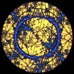
This is the second plate that had a series of patterns etched onto it in order to create different types of diffraction gratings.

These dots were made by drawing lines 5 microns wide and are the same ones shown in the first image of this blog.

This picture shows the edge of a horizontal diffraction grating.
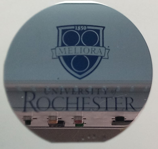
And finally this is the third plate which the universities crest was etched on.
Thanks for reading, and if you have any younger siblings interested in the camp I highly recommend it!
-ThePeculiarParticle
2 Comments
Recommended Comments