
Microelectronic Processing and Fabrication
The key to building billions of transistors on a tiny silicon wafer is to make them simultaneously in a process known as planar processing. Most microelectronic facilities begin with thin, flat, single-crystal silicon wafers of diameters ranging from 100 to 450 millimeters, with thicknesses ranging from approximately 0.5 to 1 millimeter. These silicon wafers are near-perfect crystals, with purity better than 99.9999 percent.
The microelectronic devices are created through a series of steps which include deposition of thin films of material, patterning of these thin films, selective etching of thin films, and modification of these materials. When these basic steps are repeated over and over, in a specific sequence, with varying parameters and patterns, hundreds of chips can be created on a single wafer, each chip containing hundreds of millions of functioning devices.
Looking at a single transistor in cross-section on the wafer, you can see it is made up of a p-n-p structure in the silicon, with a thin insulator above the n-type silicon region, known as the gate dielectric. Conducting contacts (typically heavily-doped poly-crystalline silicon or metals) form the source, gate, and drain regions.
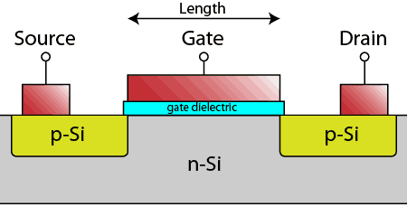
When a negative potential is placed on the conductor above the gate dielectric, the n-region in the silicon inverts to p-type and current can flow through the transistor. With no potential above the gate dielectric, the p-n-p structure blocks current flow.
In modern devices, the gate region itself is often times less than 100 nanometers in length. These devices are embedded in the silicon and then connected together in a variety of configurations with alternating layers of insulators and conductors to form a wiring scheme on top of the transistors themselves.
In a modern integrated circuit processing plant, a state-of-the-art device may require more than 400 processing steps. The fabrication process utilizes the same equipment for different steps. Even so, due to the high tech nature of the equipment and extremely clean environment in which devices are manufactured, the factory may cost upwards of $5 billion to build, with approximately $1 billion for the building, and $4 billion in equipment!
Processing steps and equipment are broken down by function. Key process groups in a modern-day wafer fabrication plant, also known as a fab, include:
- Lithography - Create Patterns
- Etch and Clean - Transfer Patterns and Remove Contaminants
- Thin Film Deposition - Deposit Materials
- Implant and Diffusion - Modify Materials
Lithography
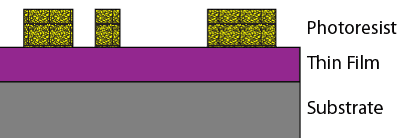
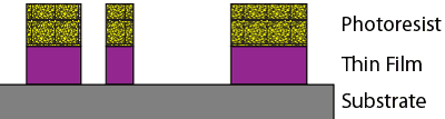
Lithography uses imaging techniques similar to photography to create tiny images on the silicon wafer. A thin layer sensitive to ultraviolet radiation known as photoresist is put on the wafer in a process known as spin coating. The wafer is placed in a bowl and a liquid solution of the photoresist is dispensed in a stream onto the wafer while the wafer spins at high speed, creating a very thin, uniform coating across the wafer.
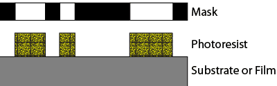
The coated wafer is then placed in an illumination system known as a stepper or scanner. The stepper or scanner shines UV radiation through a lens, through a mask (part of circuit pattern), and into the layer of photoresist coating the wafer. When the UV rays strike the photoresist, they cause a chemical reaction to take place. This is called exposure, and exposed resist will become soluble or insoluble in certain chemicals.
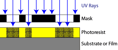
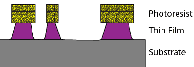
The wafer is then placed in a chemical developer, removing the regions of photoresist with high solubility and leaving the regions of photoresist with low solubility. In the example shown in the diagram, the exposed resist becomes less soluble. This is known as a negative photoresist process. Alternately, other types of photoresist become more soluble after exposure. Processes using this type of photoresist are known as positive photoresist processes.
So what's the big deal? Since the 1960s this process has been revised until you can transfer millions of patterns at once across a wafer, at feature sizes smaller than the wavelength of light.
Of course, this is simplified tremendously, and there are many variations on photoresist, developers, and steppers. Lithography is a rapidly evolving application of a variety of scientific disciplines, including, but not limited to, chemistry, optics, material science, computer programming, nuclear physics, and robotics.
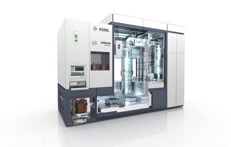
ASML's state-of-the-art Twinscan NXT:1950i lithography system, capable of imaging 38 nanometer features while printing 200 wafers per hour. Image courtesy of ASML.
Etch and Clean
Etch and Clean (oftentimes subdivided into smaller process groups) transfer lithographic patterns into the wafer and remove contaminants and other materials from the wafer. Basic processes fall into two categories: those using wet (liquid) chemicals, and those using dry (gaseous) chemicals.
Wet clean processes involve the application of liquid chemicals to clean and remove a variety of unwanted materials from the wafer. Small particles of dust and debris from the atmosphere which land on the wafer can lead to non-functioning devices, and contamination sources may be passed from machine to machine. To provide an example, a dust particle in the air may have a diameter of 2 to 200 micrometers. The length of a transistor gate can be significantly less than 0.1 microns. Since a single speck of dust can cause a device not to function, devices are fabricated in extremely clean facilities known as cleanrooms.
Wafers will be subjected to clean processes many times during the fabrication cycle, each time with the goal of leaving a pristine surface and increasing the number of functional devices on each wafer (also known as the wafer yield).
In all cases, care must be taken to remove only the unwanted material, while leaving behind the desired materials and patterns on the wafer. This requires a solid background in chemistry, material science, and robotics.
Dry and wet etch processes utilize chemicals to selectively remove material, transferring a photoresist pattern into an underlying thin film. The process begins with a thin film that has been coated with photoresist and patterned by the lithography process.
In a wet etch process, a liquid chemical which dissolves the thin film, but not the photoresist or substrate, is applied to transfer the pattern into the thin film.
The photoresist pattern is then removed, leaving behind the patterned thin film. Note that the wet etch process is isotropic, meaning it removes material in both the horizontal and vertical direction. This results in angled sidewalls and wasted space where more transistors could be fabricated.
In a dry etch process, a gaseous chemical is placed into a very strong electric field, pulling the electrons from many of the gas molecules and creating gas ions in a type of plasma known as a glow discharge. By placing a negative potential underneath the wafer, the ions can be accelerated vertically downward toward the substrate. As the ions accelerate toward the substrate, they break up the gas molecules they move through into highly reactive species, while also providing both a physical attack and a chemical attack to the thin film to be removed. This type of dry etch process is therefore known as reactive ion etching, or RIE.
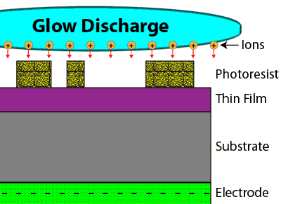
Through this effect, a dry etch process can create an anisotropic etch profile, meaning it removes materials in the vertical direction only.
Once the thin film has been patterned, the photoresist is again removed.

The dry etch process results in less wasted space on the wafer, allowing for a higher packing density of transistors, and ultimately, a cheaper and faster IC.
Both wet and dry processes and equipment require great care and precision in the design and control of IC fabrication steps. This functional group is a great area for those with an interest in chemistry, material science, physics, engineering, mechanics, and robotics.
Thin Film Deposition
Thin Film Deposition processes place thin, uniform coatings of various materials onto wafers. This can be accomplished using a variety of methods, ranging from physical vapor deposition (PVD) processes such as evaporation and sputtering to chemical deposition processes such as chemical vapor deposition (CVD) and electrochemical deposition (ECD). Each of these methods has its advantages and disadvantages, and is capable of depositing a variety of materials.
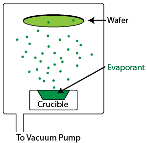
Evaporation is a physical vapor deposition process in which the wafer is placed in a chamber and subjected to very low pressures as the gases in the chamber are removed using a vacuum pump. Once the chamber is free of residual gases, the material to be deposited is subjected to a temperature sufficient to cause it to evaporate. The evaporated molecules are dispersed throughout the chamber, landing on the wafer (and the chamber walls) and condensing, coating the wafer uniformly. Evaporation is typically used for materials with high vapor pressures, such as metals, although it is also used occasionally for dielectric films such as SiO2 and MgF2, commonly used in the optics industry.
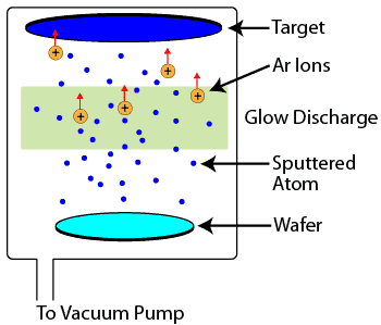
Sputtering is another physical vapor deposition process which occurs in a vacuum chamber. A large piece of the material to be deposited, known as a target, is bombarded with high energy argon ions from a glow discharge. When the argon ions strike the target, they knock off target atoms and molecules, which are then conveyed through the vacuum to the wafer, where they condense and form a thin film. Sputtering is most commonly used for depositing metal films, but, like evaporation, can also deposit insulating films with some slight process and equipment variations.
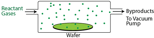
Chemical vapor deposition (CVD) can be accomplished in a vacuum (low pressure CVD, or LPCVD) or at atmospheric pressure (APCVD), although the highest quality films are deposited in a vacuum. Reactant gases are placed in a vacuum chamber with the wafer, and an energy source such as a glow discharge or infrared heating is used to activate a chemical reaction, causing the reactant gas molecules to break up, absorb on the wafer, and form a high quality thin film. CVD processes are typically used to deposit insulating and semiconducting films such as a silicon nitride (Si3N4), silicon dioxide (SiO2), tungsten (W), and polycrystalline silicon (poly-Si), though it is also capable of depositing metallic films in a process known as metal-organic CVD (MOCVD). A special type of CVD, known as atomic layer deposition, or ALD, can even deposit a single monolayer of a film at a time in a tightly controlled process.
Electrochemical deposition (ECD) is used to deposit a thin conducting copper layer which will be patterned to form interconnects (integrated wires) connecting the various devices on an integrated circuit. The wafer is submerged upside down in a conducting copper sulfate solution. In the solution, a copper electrode is connected to a power supply, which is in turn connected to the wafer, forming a circuit through the conductive solution. The negative side of the power supply is connected to the wafer, forming the cathode. The positive side of the power supply is connected to the copper electrode in the solution, known as the anode.
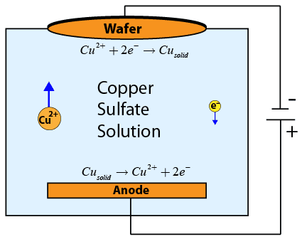
As current flows through the circuit (and through the solution), copper ions in solution near the cathode recombine with electrons from the current flow to form solid copper on the wafer.
These copper ions are replaced by copper ions produced at the anode. The process is very carefully controlled, as the amount of copper deposited is directly proportional to the amount of current flowing through the circuit!
Implant and Diffusion
The ion implantation group is responsible for introducing donor and acceptor atoms into the silicon. The exact type of dopant atom, the depth to which it is placed, and the concentration at which it is introduced are all key facets which need to be well controlled and understood to successfully manufacture an IC.
An ion implanter is a device which takes a source material and creates an ion of the desired species. The species to be implanted is selected and accelerated through a column until it collides with the wafer, embedding itself in the silicon and replacing a silicon atom in the crystal lattice with the dopant atom.
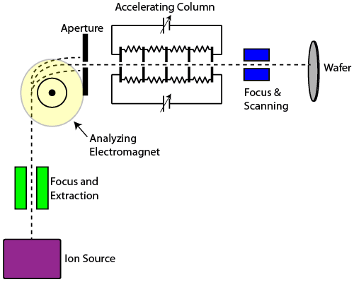
An ion source takes a gaseous species and creates a glow discharge, resulting in a large number of ions. Focus and extraction electrodes electrically pull the ions from the source into a beam. The moving ions then enter the mass analyzer, a large electromagnet which can be tuned to provide just the right force such that ions of the desired charge and mass pass through an output aperture, while ions of unwanted charge and mass are either bent too much or too little and are stopped by the aperture.
The remaining ions are then accelerated by a series of electrodes held at high potential, providing the ions with a tremendous amount of kinetic energy. The ions are then focused once more and scanned back and forth across a wafer, where they implant themselves in the silicon. If a photoresist mask is used prior to implantation, ions can be implanted in specific regions of the silicon.
Diffusion is the process by which particles spread from areas of higher concentration to lower concentration. In semiconductor manufacturing, diffusion processes are used to distribute ions which were introduced into the silicon by ion implantation throughout the silicon wafer. Because most p-type and n-type dopant ions diffuse quite slowly through silicon, the wafers are typically heated to temperatures ranging from 800 to 1200°C to speed up dopant distribution. This is accomplished through the use of a large, carefully controlled furnace designed specifically for wafer processing.
Diffusion can also modify the surface of the silicon. If silicon is placed in a high temperature furnace while in the presence of oxygen, the silicon will react with the oxygen to form a very high quality insulating layer of silicon dioxide (SiO2), more commonly known as glass. Because these layers have extremely few imperfections, this can lead to even higher quality films than those deposited using PVD or CVD processes.
Applying these basic process steps to modify, pattern, deposit and etch various materials again and again and again, each time with different parameters and patterns, allows engineers to create billions of devices simultaneously. A state-of-the-art fabrication process may contain well in excess of 400 processing steps and 30 different masks.
Once the devices have been completed on the wafer, the wafers are tested, sent to the packaging group for dicing and encapsulation, tested again, and shipped.
Defining the actual microelectronic fabrication process to create a device is known as process integration. Process integration involves combining all of the individual silicon processing steps with the appropriate masks and equipment settings to create a functioning device.