
Microelectronic Process Integration
Defining the actual microelectronic fabrication process to create a device is known as process integration. Process integration involves combining all of the individual silicon processing steps with the appropriate masks and equipment settings to create a functioning device. The simplified process flow to create an integrated resistor (shown below) provides an indication of the methods in which these steps may be combined.
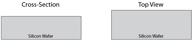
Start with Silicon Wafer
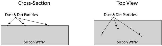
Wet Clean the Wafer
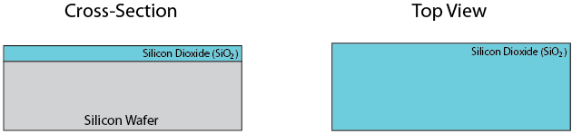
Oxidize the Wafer in Diffusion Furnace
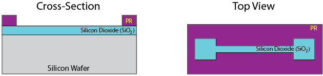
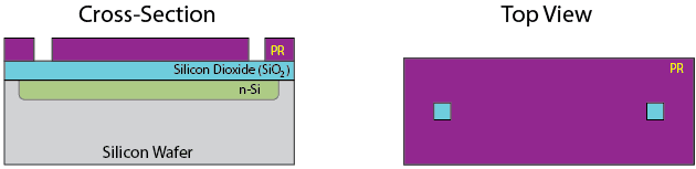
Coat, Expose, and Develop Photoresist
Dry Etch Oxide, Stop on Silicon
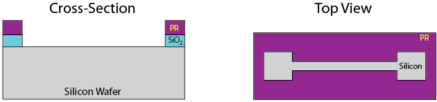
Ion Implantation into Silicon
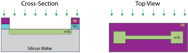
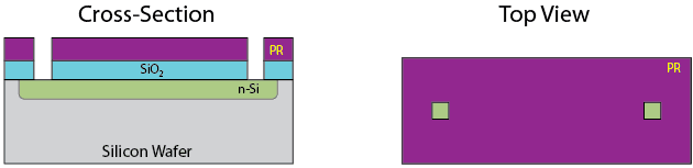
Etch Photoresist and Oxide
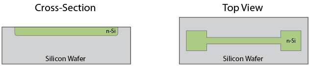
Oxidize the Wafer in Diffusion Furnace
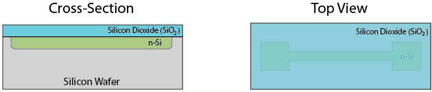
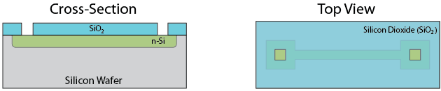
Coat, Expose, and Develop Photoresist
Coat, Expose, and Develop Photoresist
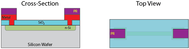
Remove Photoresist
Deposit Metal by Sputtering or Evaporation
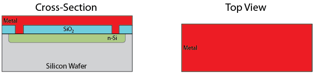
Coat, Expose, and Develop Photoresist
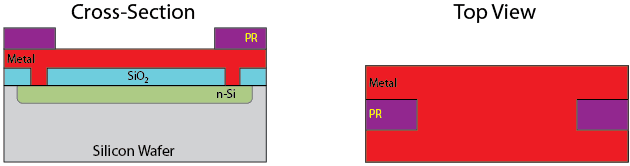
Dry Etch Metal, Stop on SiO2
Remove Photoresist
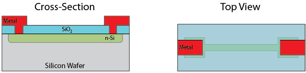
You have now created a diffused resistor in silicon. Electrical current travels through the metal and into the silicon, which has been modified to a desired conductivity by the implantation of dopant ions. The current then runs through the doped silicon and out the opposite metal contact.
Though modern devices are considerably more complex, the same basic patterning and processing steps are used in their fabrication. For an added challenge, consider building an integrated resistor or other device using a Lego model.
LEGO Diffused Resistor
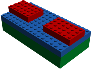
Basic instructions for a Lego diffused resistor are included here. Color code: green=silicon; orange=doped silicon; blue=oxide; red=metal. View required parts list here.